Different types of solar panels are commonly used to harvest solar energy all across the globe.
Solar panels absorbs sunlight throughout the day and convert it into electricity.
In principle, a solar panel generates electrical current by the photovoltaic effect when light particles from the sun (also known as photons) knock off excess electrons from the atoms of semiconductors.
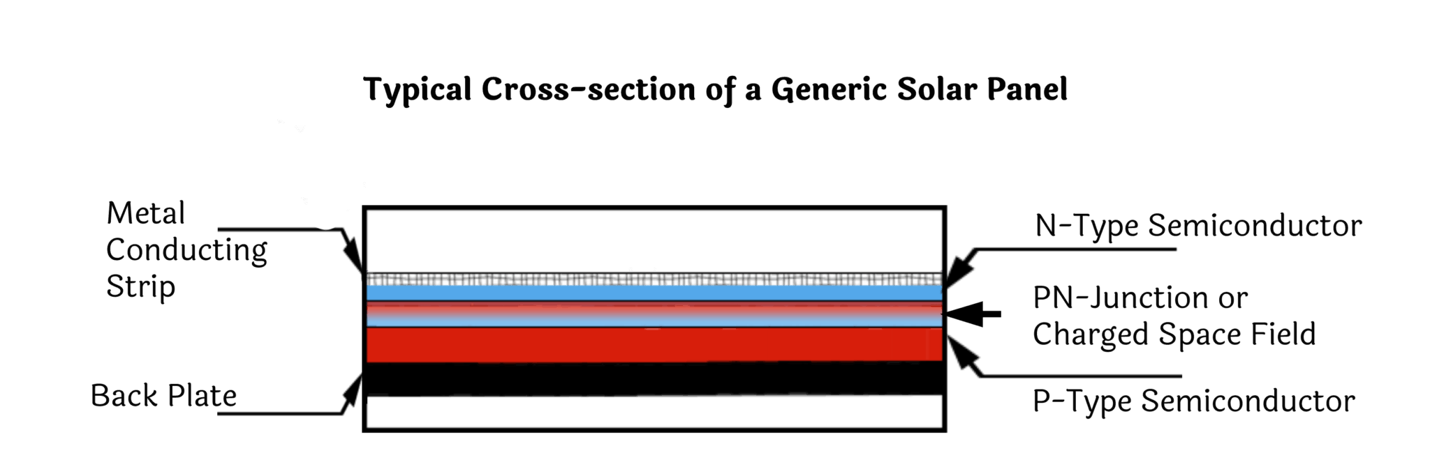
Solar Panels are made up of several cells. A single solar cell is made up of adjacent layers of n-type and p-type semiconductor. The n-type semiconductor is in contact with conducting metal strips while the p-type semiconductor is in contact of a back plate. The conducting metal strips and the back plate act as terminals for conducting electrical current.
Here, the excess electrons from the n-type semiconductor and the excess holes from the p-type semiconductor get attracted to each other and create a charged space field at the junction. This junction is called as the P-N Junction.
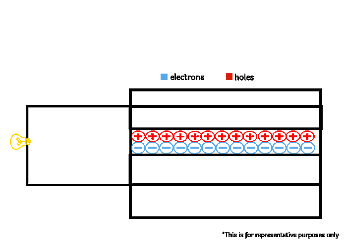
As we can see the anatomy of the cell, it can be observed that the n-type layer of semiconductor is thin in comparison to the p-type layer of semiconductor. This is to allow the light particles to reach the charged space field or the p-n junction. When light particles or photons hit the charged space field, their energy is absorbed by the electrons. These electrons are now at a higher state of energy. Eventually the threshold energy of charged space field is breached and the electrons and holes move freely.
Now, if an external load is applied to the cell from the terminals via the conducting metal strips and the back plate, the electrons start flowing in the circuit which gives rise to an electrical current (which is in the opposite direction of the electron flow). Due to opposite polarity, the electrons get attracted to the holes and re-enter the circuit via the back plate and return to the state of electrical neutrality.